- 您现在的位置:买卖IC网 > Sheet目录366 > TMDXEVM5515 (Texas Instruments)EVAL MODULE DSP FOR C55XX
�� ���
���
���SPRS645F� –� AUGUST� 2010� –� REVISED� OCTOBER� 2013�
�2.5.12� SAR� ADC� Terminal� Functions�
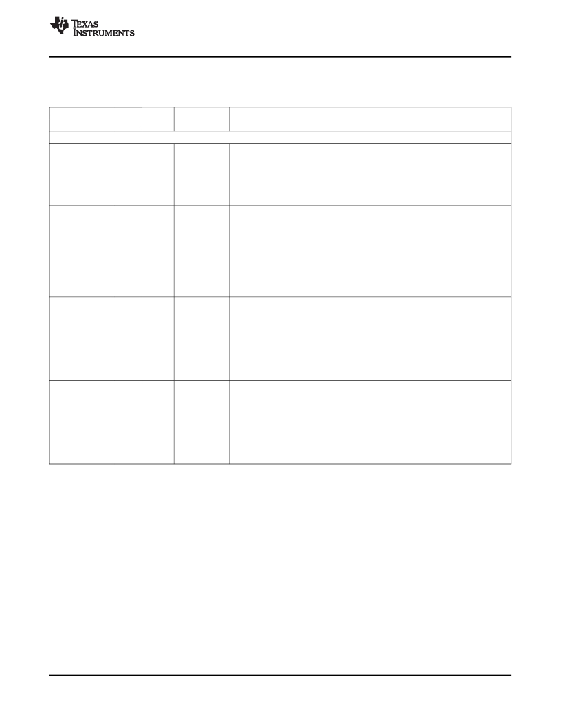
�Table� 2-17.� 10-Bit� SAR� ADC� Terminal� Functions�
�SIGNAL�
�NAME�
�NO.�
�TYPE� (1)�
�(2)�
�OTHER� (3)�
�(4)�
�DESCRIPTION�
�SAR� ADC�
�GPAIN0:� General� -Purpose� Output� and� Analog� Input� pin� 0.� This� pin� is� demuxed�
�internally� into� ADC� Channels� 0,� 1,� &� 2.� GPAIN0� can� also� be� used� as� a� general-�
�purpose� open-drain� output.� This� pin� is� unique� among� the� GPAIN� pins� in� that� it� is� the�
�GPAIN0�
�D10�
�I/O�
�V� DDA_ANA�
�only� pin� that� is� 3.6� V-tolerant� to� support� measuring� a� battery� voltage.� GPAIN0� can�
�accommodate� input� voltages� from� 0� V� to� 3.6� V;� although,� the� ADC� is� unable� to�
�accept� signals� greater� than� V� DDA_ANA� without� clamping.� ADC� Channel� 1� is� capable�
�of switching in an internal resistor divider that has a divide ratio of approximately 1/8.�
�GPAIN1:� General� -Purpose� Output� and� Analog� Input� pin� 1.� This� pin� is� connected� to�
�ADC� Channel� 3.� GPAIN1� can� be� used� as� a� general-purpose� output� if� certain�
�requirements� are� met� (see� the� following� note).� GPAIN1� can� accommodate� input�
�voltages� from� 0� V� to� V� DDA_ANA� .�
�GPAIN1�
�A11�
�I/O�
�V� DDA_ANA�
�Note:� If� the� ANA_LDO� is� used� to� supply� power� to� V� DDA_ANA� ,� this� pin� must� not� be�
�used� as� a� general-purpose� output� (driving� high)� since� the� max� current� capability�
�(see� the� I� SD� parameter� in� Section� 4.3� ,� Electrical� Characteristics� Over� Recommended�
�Ranges� of� Supply� Voltage� and� Operating� Temperature� )� of� the� ANA_LDO� can� be�
�exceeded.� Doing� so� may� result� in� the� on-chip� power-on� reset� (POR)� resetting� the�
�chip.�
�GPAIN2:� General� -Purpose� Output� and� Analog� Input� pin� 2.� This� pin� is� connected� to�
�ADC� Channel� 4.� GPAIN2� can� be� used� as� a� general-purpose� output� if� certain�
�requirements� are� met� (see� the� following� note).� GPAIN2� can� accommodate� input�
�voltages� from� 0� V� to� V� DDA_ANA� .�
�GPAIN2�
�B11�
�I/O�
�V� DDA_ANA�
�Note:� If� the� ANA_LDO� is� used� to� supply� power� to� V� DDA_ANA� ,� this� pin� must� not� be�
�used� as� a� general-purpose� output� (driving� high)� since� the� max� current� capability�
�(see� the� I� SD� parameter� in� Section� 4.3� ,� Electrical� Characteristics� Over� Recommended�
�Ranges� of� Supply� Voltage� and� Operating� Temperature� )� of� the� ANA_LDO� can� be�
�exceeded.� Doing� so� may� result� in� the� on-chip� POR� resetting� the� chip.�
�GPAIN3:� General� -Purpose� Output� and� Analog� Input� pin� 3.� This� pin� is� connected� to�
�ADC� Channel� 5.� GPAIN3� can� be� used� as� a� general-purpose� output� if� certain�
�requirements� are� met� (see� the� following� note).� GPAIN3� can� accommodate� input�
�voltages� from� 0� V� to� V� DDA_ANA� .�
�GPAIN3�
�C11�
�I/O�
�V� DDA_ANA�
�Note:� If� the� ANA_LDO� is� used� to� supply� power� to� V� DDA_ANA� ,� this� pin� must� not� be�
�used� as� a� general-purpose� output� (driving� high)� since� the� max� current� capability�
�(see� the� I� SD� parameter� in� Section� 4.3� ,� Electrical� Characteristics� Over� Recommended�
�Ranges� of� Supply� Voltage� and� Operating� Temperature� )� of� the� ANA_LDO� can� be�
�exceeded.� Doing� so� may� result� in� the� on-chip� POR� resetting� the� chip.�
�(1)�
�(2)�
�(3)�
�(4)�
�I� =� Input,� O� =� Output,� Z� =� High� impedance,� S� =� Supply� voltage,� GND� =� Ground,� A� =� Analog� signal,� BH� =� Bus� Holder�
�Input� pins� of� type� I,� I/O,� and� I/O/Z� are� required� to� be� driven� at� all� times.� To� achieve� the� lowest� power,� these� pins� must� not� be� allowed� to�
�float.� When� they� are� configured� as� input� or� high-impedance� state,� and� not� driven� to� a� known� state,� they� may� cause� an� excessive� IO-�
�supply� current.� Prevent� this� current� by� externally� terminating� it� or� enabling� IPD/IPU,� if� applicable.�
�IPD� =� Internal� pulldown,� IPU� =� Internal� pullup.� For� more� detailed� information� on� pullup/pulldown� resistors� and� situations� where� external�
�pullup/pulldown� resistors� are� required,� see� Section� 3.8.1� ,� Pullup/Pulldown� Resistors� .�
�Specifies� the� operating� I/O� supply� voltage� for� each� signal�
�Copyright� ?� 2010–2013,� Texas� Instruments� Incorporated�
��Product� Folder� Links:� TMS320C5515�
�Device� Overview�
�37�
�发布紧急采购,3分钟左右您将得到回复。
相关PDF资料
TMDXEXP1808L
KIT EXPERIMENTER FOR AM180X
TO263-3EV-VREG
BOARD EVAL TO220-3/TO263-3 VREG
TO263-5EV-VREG
EVAL BOARD VREG TO220-5/TO263-5
TOOLSTICK-EK
KIT TOOL EVAL SYS IN A USB STICK
TPS23757EVM
EVALUATION MODULE FOR TPS23757
TPS62230EVM-370
EVAL MODULE FOR TPS62230-370
TRAVELCUBE
SURGE SUP 1OUT W/RJ11 DIRECTPLUG
TRAVELER100BT
SURGE SUP 2OUT W/RJ11 DIRECTPLUG
相关代理商/技术参数
TMDXEVM5515
制造商:Texas Instruments 功能描述:TMS320C5515 DSP Evaluation Module
TMDXEVM642
制造商:Texas Instruments 功能描述:Tools Development kit For Use
TMDXEVM6424
功能描述:开发板和工具包 - TMS320 C6424 DSP Eval Mod RoHS:否 制造商:Texas Instruments 产品:Experimenter Kits 工具用于评估:F2802x 核心:TMS320 接口类型:UART, USB 工作电源电压:
TMDXEVM6446
制造商:Rochester Electronics LLC 功能描述:DAVINCI EVM BUNDLE W/O EMULATOR - Bulk 制造商:Texas Instruments 功能描述:DAVINCI EVM BUNDLE W/O EMULATOR - Bulk
TMDXEVM6446T
制造商:Texas Instruments 功能描述:DM6446 DIGITAL VIDEO EVALUATION MODULE - Boxed Product (Development Kits)
TMDXEVM6446TS
制造商:Texas Instruments 功能描述:DM6446 DIGITAL VIDEO EVALUATION MODULE - Trays
TMDXEVM6452
功能描述:开发板和工具包 - TMS320 C6452 EVM Evaluation Module RoHS:否 制造商:Texas Instruments 产品:Experimenter Kits 工具用于评估:F2802x 核心:TMS320 接口类型:UART, USB 工作电源电压:
TMDXEVM6455
功能描述:开发板和工具包 - TMS320 C6455 Evaluation Module RoHS:否 制造商:Texas Instruments 产品:Experimenter Kits 工具用于评估:F2802x 核心:TMS320 接口类型:UART, USB 工作电源电压: